Japan Establishes New Method for Efficient Production of Monocrystalline Silicon
 |
The principle of NOC growth method
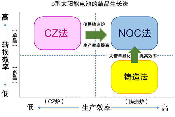
The positioning of NOC growth method
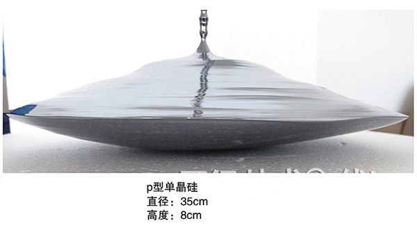
Monocrystalline silicon ingots made using the NOC method have a protruding growth interface below
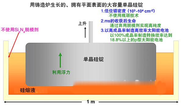
Example of growth of large-bore, high-capacity single-crystal silicon ingots through a large crucible using the NOC method
The Japan Science and Technology Agency (JST) announced on August 9, 2016 that it has developed a new method for producing single-crystal silicon using a high-efficiency casting growth furnace and uses solar energy of single-crystal silicon ingots manufactured based on this method. The conversion efficiency of the battery reached 19.14%. By using monocrystalline silicon manufactured using a cast growth furnace, the same level of high efficiency and high yield as that of a monocrystalline solar cell manufactured by the Czochralski single crystal manufacturing process (CZ method) is achieved.
For silicon wafers for solar cells, the production of polysilicon using a cast-growth furnace is more efficient and less expensive than monocrystalline silicon produced using a CZ growth furnace, so that 60% of the solar cell market is occupied by polysilicon. However, there are two problems with polysilicon. First, when an excellent polycrystalline structure is formed, the crystal quality deteriorates. Therefore, the conversion efficiency is lower by 1 to 1.5% than that of single crystal silicon. Second, there is residual deformation, and therefore the quality of the crystal is not uniform. Larger, low yield.
The non-contact niobium method (NOC method) developed this time uses a foundry growth furnace for producing polycrystalline silicon ingots, and ingeniously sets a low-temperature zone in the melt, allowing single crystal growth without contacting the niobium wall ( The original experience used to form low temperature areas was not disclosed). The graphite jigs as the contents of the growth furnace were all burned in a vacuum at high temperature for a long time to remove impurities. In addition, the crystal dislocation and oxygen concentration are reduced by reducing the rising speed and rotation speed of the single crystal in the growth as much as possible, and the crystal defects are reduced.
This time, the p-type single-crystal silicon ingot obtained by the above method was used to uniformly cut wafers from all regions, and a prototype of the Al-BSF (aluminum back-field) solar cell was fabricated using the wafer, resulting in a very high yield. High-efficiency solar cells with a maximum conversion efficiency of 19.14% and an average conversion efficiency of 19.0% are realized. In addition, a single crystal silicon ingot with a diameter ratio of 90% of the crucible diameter was successfully produced. In the future, if large-capacity single-crystal silicon ingots can be manufactured using larger crucibles, this technology is expected to become the mainstream of the solar cell market.
The related results will be announced on August 12, 2016 at the "ICCGE-18 (18th International Conference on Crystal Growth and Epitaxy)" held in Nagoya. (Special Contributor: Kudosuke)
Ventilation Hose Duct,Flexible Drain Hose,2 Inch Suction Hose,Rail Ventilation Hose
Changxing VACUFLEX Hose Technology Co., Ltd. , https://www.vacuflex-cn.com