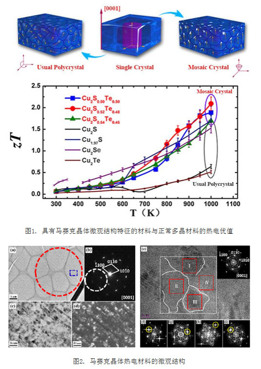
With the increasingly prominent environmental and energy issues, the development and utilization of new clean energy technologies have attracted the attention of countries. In addition to the green energy such as solar energy and wind energy, there is still a huge amount of energy in the nature and human activities. Waste heat is not effectively recycled. New clean energy technologies based on thermoelectric conversion materials can convert these low-quality thermal energy recycling into useful electrical energy, with significant advantages such as zero emissions, safety and reliability, and a wide range of operating temperatures. The large-scale commercialization of thermoelectric energy conversion technology is first subject to the properties of the material, which is determined by the electro-thermal transport of the material. Thermoelectric materials with superior performance need to satisfy the intrinsic conflicting requirements of excellent electrical transport and extremely low heat conduction at the same time. In monocrystalline materials, the highly complete lattice has low scattering of carriers and phonons, resulting in extremely high conductivity and thermal conductivity. When materials are transformed from single crystals to polycrystals, there are a large number of polycrystalline materials with random distributions of grain size and grain orientation. Electro-thermal transport is scattered by grain boundaries and randomly oriented, and its electrical conductivity and thermal conductivity are large. Reduced in magnitude. However, when the grain size of the polycrystalline material is reduced to the nanometer level, an order of magnitude increased interface produces strong scattering of carriers and phonons, resulting in a very low electrical conductivity and thermal conductivity of the material. The realization of synergistic or independent regulation of electricity and heat in the same material is a key and difficult problem affecting thermoelectric performance, which directly determines the energy conversion efficiency of the thermoelectric technology. For different material systems, the optimization of thermoelectric properties depends on the adjustment and control of the microstructure of the material, and the coordinated control of the electric heat transport is achieved to achieve maximum electric transport and low heat conduction. Recently, researchers from Shanghai Institute of Ceramics, Chinese Academy of Sciences Shi Xun, Xu Wei, and Chen Lidong collaborated with University of Michigan professor Uher and Northwestern University professor Snyder to successfully synthesize a polycrystalline material that is different from the ordinary grain-oriented random polycrystalline materials. The grain-free monocrystalline material and the highly oriented mosaic crystal thermoelectric material achieve extremely low thermal conductivity similar to the glass material and excellent electric transport performance of the crystal material, and its thermoelectric value zT reaches 1000 K. 2.1 (see Figure 1) is much higher than that of ordinary polycrystalline material systems. The mosaic crystal is a very special material state and appears to be a highly perfect single crystal macroscopically, but in fact it is composed of many nanometer-sized perfect small crystals with slight angle deflection. Unlike the random distribution of lattice orientation in ordinary polycrystalline or nanocrystalline materials, the angle of deflection of the mosaic grains is so small that it appears to be almost a single crystal, which also results in the presence of numerous small-angle grain boundaries in the material. In terms of the effect of electro-thermal transport, the highly-aligned grain orientation of the single crystal can result in excellent electrical transport of the material, while the small angular shift of the mosaic grains can strongly affect the heat transfer. Therefore, a material having a mosaic crystal microstructure has extremely excellent thermoelectric properties. The traditional mosaic crystal is generally prepared by the flash cooling method, ie, the material is heated to a high temperature, and ultra-fast cooling is used to force the defects in the structure to not spread to the surface of the material and accumulate to form a mosaic grain boundary. The conditions for forming a mosaic crystal are sufficiently fast cooling rates, which also leads to the current research of mosaic crystals generally limited to high thermal conductivity materials such as metals, diamonds or some oxides. However, the thermal conductivity of thermoelectric materials is generally very small, and a sufficiently fast cooling rate cannot be obtained. Therefore, the study of thermoelectric materials having a mosaic crystal microstructure has been a gap. The Shanghai Silicate Research Institute has found that by using the traditional solid-state reaction method, a huge mismatch of the atomic masses and atomic radii of S and Te anions can be used in Cu2S1-xTex solid solutions to realize mosaic crystals in bulk thermoelectric materials. micro structure. Based on the previous research on Cu2X (X = S, Se, Te) (Adv. Mater. 2014, 26, 3974; Adv. Mater. 2013, 25, 6607; Nat. Mater. 2012, 11, 422), researchers A very abnormal complete solid solution compound Cu2(S, Te) was obtained. Unlike Cu2S and Cu2Te, which have an unusually complex crystal structure at room temperature, the Cu2(S, Te) solid solution is a single-phase material at room temperature and has a highly symmetrical hexagonal crystal structure (P63/mmc), which is the same as the Cu2S intermediate temperature structure (b -Cu2S). SEM and EBSD observations revealed that the solid solution was a polycrystalline material with a wide crystal grain size distribution range (90 nm to 6 mm) and an arbitrary crystal grain orientation. The elemental scan analysis was performed on the SEM and TEM scales. Its constituent elements are uniformly distributed and no second phase exists. The ultra-thin sections of the solid-solution samples and the TEM observations of the powders revealed that the microstructure of the single crystal grains of the solid-solubilized compound exhibited special mosaic crystal characteristics: the inside of a single crystal grain is composed of subgrains of a size of 10-20 nm in size. (See Fig. 2(c)(d)), these sub-crystals are nearly uniform in orientation and show the same diffraction pattern (see Fig. 2(e)), while the sub-grains have extremely small angular deflections and behave the same. There are differences in the brightness of the different diffraction spots in the diffraction pattern (see Fig. 2(fi)). After 973 K high temperature, the features of the mosaic crystal structure remain. The optimal combination of high-temperature electric and heat transport parameters was achieved by compositional regulation. Conductivity was in the range of 104 Ω-1 m-1 for 300 K-1000 K, and the Seebeck coefficient was in the 60 μV K-1 to 260 μV K-1 range. The total thermal conductivity is as low as 0.8 W m-1 K-1 in the entire measurement temperature range, which shows a clear competitive advantage over other material systems. In addition, the fitting analysis of electro-acoustic scattering and single paraboloid band approximation for high-temperature electric transport shows that the Seebeck coefficient of the solid solution sample has a significant increase relative to the matrix material, possibly with a large number of nanometer scales in its special mosaic crystal structure. The interface is related to quantum effects or energy filtering effects. The measurement of the low-temperature heat transport of this solid solution sample has also found a very interesting phenomenon. Although this material is a polycrystalline material, its low-temperature thermal conduction behavior exhibits the heat transfer characteristics of the amorphous glass, ie, its lattice heat. The relationship between conductivity and temperature shows that no characteristic peak appears in the crystalline material in the low temperature region near 10-50 K, and the lattice thermal conductivity value is very low, and the low temperature range of 2 K-300 K is crystal. The thermal conductivity of lattice is lower than 0.5 W m-1 K-1, even lower than the thermal conductivity of amorphous glass. It may come from the limitation of the average free path of heat transfer phonons in the numerous nano-interfaces in the microstructure. The effect is similar to the effect of lattice long-range disorder in amorphous glass. Different from the previous optimization methods of electricity or heat used in thermoelectric materials, Cu2S and Cu2Te form a solid solution sample Cu2(S, Te) to achieve the simultaneous optimization of electrical transmission and heat conduction, that is, through the microstructure design breaks The coupling relationship between electricity and heat transport parameters, if combined with other existing optimization methods, such as energy band engineering, is expected to further improve its thermoelectric performance. The microstructure with mosaic crystal features is a new method of thermoelectricity control, which provides a new direction and solution for the optimization and application of thermoelectric materials. The relevant research was published in "Advanced Materials, adma. 201501030R1". The research work was funded and supported by the National Basic Research "973" project and the National Natural Science Foundation. Drill Nut,Threaded Hex Drill Anchor Nuts,Domed Coupling Drill Nuts,Domed Drill Anchor Nuts J.B Machinery (Ningbo) Co., Ltd. , https://www.jbdrill.com